Collect
Industrial
 Navigateㄩ
What kind of knowledge does the photoelectric sensor need to know?
The electro-optical control panel is such a converter that converts changes in the amount of light into changes in power consumption. It has been widely used and has been used in aerospace, Chinese medicine, scientific research, industrial control, home appliances, and shipping. The basic knowledge of photoelectric sensors is based on the photoelectric effect, and various photoelectric sensors can be produced according to the photoelectric effect. Today, the basic basic knowledge of the photoelectric effect is explained in detail for everyone. In the early days, the photoelectric effect was made into photocells. Its design and construction are shown in the figure below. It is a vacuum-crystallized glass crystal bubble with a metal-coated composite or hydroxide on the inner wall of the bubble as a negative level of the phototube. The anode treatment of the phototube is a metal composite ball of the ring-shaped fine iron wire or semi-circular elemental element.
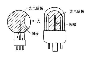
Photocell structure
The experimental equipment for the photoelectric effect is shown in the figure below. The anode treatment A of the photocell is connected to a high potential, and the negative K is connected to a low potential difference. Then, there is an accelerating electric field between the anode treatment and the negative phase, and the electric field direction is biased by K by A. The operating frequency in the middle of the AK is loaded by the galvanometer V, and the specification of the operating frequency is derived from the varistor R. In the figure, G is a smart current meter. The experiment pays attention to the fact that when the negative stage is not exposed to light, most of the switching power supply principle has no current value; when the negative stage is exposed to light, the current value appears immediately in the switching power supply principle. How long does the light last? How long does the current value last? When the light stops, the current value dissipates. This means that when the light is illuminated, electronic components escape from the electron optical negative level. Under the action of the accelerating electric field, the electronic components fly to the anode to cause photocurrent in the control circuit.
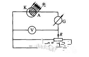
Photoelectric effect experimental equipment
The compound releases electronic components under the action of light, a condition called photoelectric effect. Photoelectric effect is usually divided into two categories: external photoelectric effect and internal photoelectric effect.
Photoelectric effect
External photoelectric effect
Under the action of the light source, the electronic components in the block escape the surface of the block, and the outward emission point is called the external photoelectric effect. The semiconductor device according to the external photoelectric effect has a photo transistor, a photomultiplier tube, and the like.
2. Internal photoelectric effect
The error between the two lines of the illuminated block changes, or the effect of the photogenerated electromotive force is called the internal photoelectric effect. The internal photoelectric effect can be further divided into the following two categories.
1) Electron optical guiding effect
Under the action of the light source, the electronic component digests the photon beauty machine to connect to the casual condition from the bonding condition, resulting in a change in the material resistor. This condition is called electron optical guiding effect. Most high-resistance semiconductor devices have an electron optical guiding effect. The semiconductor device according to this effect has a photoresistor (also called an electro-optical plastic hose), and its common raw materials are cadmium sulfide (CdS), lead sulfide (PbS), indium antimonide (InSb), amorphous silicon (a- Si: H), etc.
In the pure semiconductor device, under the illumination of the light source, the electronic components in the forbidden band are excited by the photon beauty whose mechanical energy exceeds or equals the forbidden band width Eg(eV), and the valence band passes over the forbidden band free electrons to the conduction band and becomes Free electronics. Together, the price band also caused casual cavitation. The concentration of cavitation mass of the electronic components and the valence band of the conduction band in the pure semiconductor device is expanded, and the resistor of the semiconductor device is lowered. Figure (a) shows the legend. Electronic components and cavitation are collectively referred to as carriers. They can cause photocurrent under the action of terminal voltage. When the light stops, the free electrons are captured by the molecular structure of the missing electronic components, and the varistor repairs the original value of the fixed assets. The valence band electronic components can be freely electroned into the spectrum analyzer layer of the conduction band, and its large optical wavelength 竹0 (nm) is called the cutoff wavelength, 竹0 > 1240 / Eg.
In the case of N-type or P-type hetero semiconductor devices, if the photon cosmetic mechanical energy exceeds the donor level and the conduction band bottom level, respectively, or the main level and the full-band top level, Ei(eV), the graph is obtained. In (b) or (c), the light energy is digested to excite photonic electronic components or cavitation that can sign up for conductivity. The doped semiconductor device causes the cutoff wavelength of the photogenerated carriers to be 竹0 > 1240 / Ei.
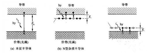
Schematic diagram of electronic optical guiding effect circuit
When the photoresistor is connected to the alternating current Vb and the common source of the tensile strength and the wavelength of the light is less than 竹0, the output AC voltage i0 is
In the formula, the quantum efficiency of 灰 is high (the ratio of photogenerated carriers to the number of photon photons); 米c〞the mobility of most carriers; 而〞the majority of carrier lifetime; d 〞〞The distance between the two levels of the photoresistor; p〞〞the power of the light source; e〞the Planck constant, which is 6.6261℅10-34J s.
With the increase of light energy, although the mass concentration of photogenerated carriers is also proliferating, the speed of recombination between electronic components and cavitation is also accelerated, so the photodynamic energy lower than the cutoff wavelength and the photocurrent caused by the semiconductor The characteristic trend graph is nonlinearly related.
2) Photovoltaic volts (such as semiconductor devices)
The case where an electromotive force in a certain direction can be caused by irradiation of light is called a photovoltaic effect. base. The semiconductor devices for this effect are photocells, photodiodes, and phototransistors.
The photovoltaic effect can be divided according to the basic principle of causing the potential difference:
Lateral photovoltaic effect
The lateral photovoltaic effect is also known as the Dember effect.
When the optically sensitive surface of a semiconductor device semiconductor device is unevenly illuminated by light, the photoelectric effect caused by the carrier concentration gradient is called a side photovoltaic effect. A semiconductor device that operates according to this effect has a semiconductor device position sensitive electronic device (collectively called PSD), or a rotating photodiode.
The basic principle of the work of the lateral photovoltaic effect is that the mechanical energy of the semiconductor device absorbs the photon of the human photon to cause the cavitation of the electronic component, so that the mass concentration of the carrier is higher than that of the unexposed part, thus the concentration occurs. The gradient causes the diffusion of carriers. Since the mobility of electronic components is larger than that of cavitation, electronic components are initially diffused to the unexposed portions, causing the illuminated portions to be positively charged, and the unexposed portions to be negatively charged, and the two portions are causing the photoelectromotive force in the middle.
PN junction photovoltaic effect
When the light is directly incident on the surface of the semiconductor device PN which is close to the surface, the junction and nearby semiconductor devices digest the light energy. If the photon beauty machine can exceed the forbidden band width, the valence band electronic components will be free electrons to the conduction band and become free electrons, while the valence band will become casually cavitation. Under the action of the electric field inside the PN junction, the electronic components are tuned to the two sides of the N-zone, and the cavitation is tuned to both sides of the P-zone. As a result, the P-zone is positively charged and the N-zone is negatively charged, causing photoelectromotive force.
The PN junction photocurrent value is proportional to the human illuminance, and the photovoltaic volt is mostly proportional to the illuminance.
Since the photo-generated electronic components and cavitation are combined with the cavitation of the semiconductor device and the electronic components during the diffusion process, the lifetime of the carriers is related to the diffusion length. Only by making the thickness of the PN junction surface smaller than the diffusion length can cause photocurrent to cause photovoltaic. In the construction project, the method of changing the thickness of the PN junction surface can be used to adjust the phase-frequency characteristics, photocurrent and photo-potential difference specifications of the semiconductor device according to the PN junction photo-voltaic effect.
Semiconductor devices according to this effect include photovoltaic cells, solar cells, photodiodes, and phototransistors. According to the scheme design and production and processing technology, the photovoltaic cell works without external power, and then works with the solar power station effect. When the photo-sensing tube is biased in the opposite direction, there is a light guiding effect and a solar power station effect. The photocurrent they output is linearly related to the light intensity.
Electron optical magnetic effect (collectively called PEM effect)
When a semiconductor device is irradiated with strong light and a magnetic field is applied in the vertical direction of the illumination, a situation in which a potential difference is caused between the two sides of the semiconductor device that vertically splits the light and the magnetic field is called an electro-optical magnetic effect. It can be used as a Hall effect that is a value of light diffusion current.
Becquerel effect
The Becquerer effect is a photovoltaic effect in a liquid. When the light is irradiated to any one of the two identical electric levels in the lithium battery electrolyte, the case where the potential difference is caused between the two electric levels is referred to as the Becquerer effect. According to this effect, there is a photosensitive battery.
PreㄩWhat is the development of sensors? 2026-06-11
NextㄩPacifier biosensor monitors newborn health 2026-06-11