Collect
 Navigate:
ALLEGRO 原装 A8904 提供技术资料(PDF文档) 咨询热线:0755-33062500
【产品名称】 A8904
【产品封装】 24-pin batwing SOIC,24-pin batwing SOIC; Lead-free,28-pin SSOP with Exposed Thermal Pad,24-pin SSOP with Exposed Thermal Pad; Lead-free
【产品类别】 无刷电机驱动芯片
【生产厂家】 ALLEGRO
【技术参数】 A8904 技术参数下载
【产品应用】 绣花机、打印机、刻字/雕刻机、生化分析仪、扫描仪、稅票机等
【产品说明】 原装 详情请来电咨询!
8904
3-PHASE BRUSHLESS DC MOTOR
CONTROLLER/DRIVER WITH BACK-EMF SENSING
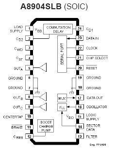
The A8904SLB and A8904SLP are three-phase brushless dc motor
controller/drivers designed for applications where accurate control of highspeed
motors is required. The three half-bridge outputs are low on-resistance
n-channel DMOS devices capable of driving up to 1.2 A. The A8904 provides
complete, reliable, self-contained back-EMF sensing, motor startup and
running algorithms. A programmable digital frequency-locked loop speed
control circuit together with the linear current control circuitry provides
precise motor speed regulation.
A serial port allows the user to program various features and modes of
operation, such as the speed control parameters, startup current limit, sleep
mode, direction, and diagnostic modes.
The A8904 is fabricated in Allegro’s BCD (Bipolar CMOS DMOS)
process, an advanced mixed-signal technology that combines bipolar, analog
and digital CMOS, and DMOS power devices. The A8904SLB is provided in
a 24-lead wide-body SOIC batwing package. The A8904SLP is provided in a
thin (<1.2 mm), 28-lead SSOP package with an exposed thermal pad. Each
package type is available in a lead-free version (100% matte tin leadframe).
Absolute Maximum Ratings
Load Supply Voltage, VBB . . . . . . . . . . . . 15 V
Output Current1, IOUT . . . . . . . . . . . . . . . . . . . . . ±1.4 A
Peak Output Current (Brake)2, IOUT(BRK) . ±3.0 A
Period2 for IOUT(BRK) to fall from
±3.0 A to ±1.4 A . . . . . . . . . . . . . . . 800 ms
Logic Supply Voltage, VDD . . . . . . . . . . . 7.0 V
Logic Input Voltage Range, VIN
(continuous) . . . . . . -0.3 V to VDD + 0.3 V
(tw <30 ns) . . . . . . . -1.0 V to VDD + 1.0 V
Package Power Dissipation, PD . . See Graph
Operating Temperature, TA . . . -20°C to +85°C
Junction Temperature3, TJ . . . . . . . . . +150°C
Storage Temperature,TS . . . . -55°C to +150°C
1Output current rating may be restricted to a value
determined by system concerns and factors. These
include: system duty cycle and timing, ambient
temperature, and use of any heatsinking and/or forced
cooling. For reliable operation, the specified maximum
junction temperature should not be exceeded.
2Peak output current is a transient condition that
occurs during braking when the motor acts as a
generator. The 3 A level is based on the maximum
peak of a sine wave that is damped. The maximum
period between the initial brake being applied and the
current through the drivers falling to 1.4 A should not
exceed 800 ms. See Braking section for more
information.
3Fault conditions that produce excessive junction
temperature will activate device thermal shutdown
circuitry. These conditions can be tolerated, but should
be avoided.
Features
Pin-for-pin replacement for A8902CLBA
Startup commutation circuitry
Sensorless commutation circuitry
Option of external sector data tachometer signal
Option of external speed control
Oscillator operation up to 20 MHz
Programmable overcurrent limit
Transconductance gain options: 500 mA/V or 250 mA/V
Programmable watchdog timer
Directional control
Serial Port Interface
TTL-compatible inputs
System diagnostics data out ported in real time
Dynamic braking through serial port or external terminal
此类产品本公司大量原装现货热卖
询价热线:
0755-83283733, 83031813,33062500
QQ:623069669
MSN:sumzi003@sumzi.com sumzi006@sumzi.com
Email:sumzi@sumzi.com
http://www.sumzi.com
Pre:高性能和低功耗Blackfin处理器用于第一个海底天然气管道监测系统设计 2026-02-08
Next:直流无刷电动机驱动器、直流电刷电动机驱动器 咨询热线:0755-33062500 2026-02-08