Collect
Industrial
 NavigateŁş
What is MOS tube? MOS tube structure principle diagram (application _ advantage _ three poles representative)
What is a mos tube
The mos tube is a metal-oxide-semiconductor field effect transistor, or a metal-insulator-semiconductor. The source and drain of the MOS tube can be reversed. They are all N-type regions formed in the P-type backgate. In most cases, the two zones are the same, even if the two ends are reversed, it will not affect the performance of the device. Such devices are considered to be symmetrical.
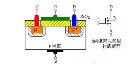
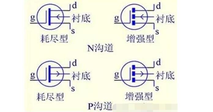
The bipolar transistor amplifies a small change in the current at the input and outputs a large current change at the output. The gain of a bipolar transistor is defined as the ratio of the output to the input current (beta). Another type of transistor, called a field effect transistor (FET), converts the change in input voltage into a change in output current. The gain of the FET is equal to its transconductance, defined as the ratio of the change in output current to the change in input voltage. Commonly used in the market are N-channel and P-channel. For details, refer to the picture on the right (N-channel depletion MOS transistor). The common P-channel is a low-pressure mos tube.
The FET affects the current flowing through the transistor by projecting an electric field on an insulating layer. In fact no current flows through this insulator, so the GATE current of the FET tube is very small. The most common FET uses a thin layer of silicon dioxide as an insulator under the GATE pole. Such a transistor is called a metal oxide semiconductor (MOS) transistor, or a metal oxide semiconductor field effect transistor (MOSFET). Because MOS tubes are smaller and more power efficient, they have replaced bipolar transistors in many applications.
Mos tube advantage
1. Can be applied to zoom in. Since the input impedance of the FET amplifier is high, the coupling capacitor can have a small capacity and it is not necessary to use an electrolytic capacitor.
2. Very high input impedance is ideal for impedance transformation. Commonly used in the input stage of multi-stage amplifiers for impedance transformation.
3. Can be used as a variable resistor.
4. Can be conveniently used as a constant current source.
5. Can be used as an electronic switch.
6. Flexibility in circuit design. The gate bias can be positive or negative and zero, the transistor can only operate under forward bias, and the tube can only operate under negative bias. In addition, the input impedance is high, which can reduce the signal source load and is easy to match with the previous stage.
MOS tube structure principle diagram
1, structure and symbol (take N-channel enhancement as an example)
Two higher-concentration N-type regions are diffused as a drain and a source on a lower concentration of P-type silicon, and the semiconductor surface covers the silicon dioxide insulating layer and leads an electrode as a gate.
What is MOS tube? MOS tube structure principle diagram (application _ advantage _ three poles representative)
Other MOS tube symbols
What is MOS tube? MOS tube structure principle diagram (application _ advantage _ three poles representative)
2, the working principle (take N-channel enhanced type as an example)
What is MOS tube? MOS tube structure principle diagram (application _ advantage _ three poles representative)
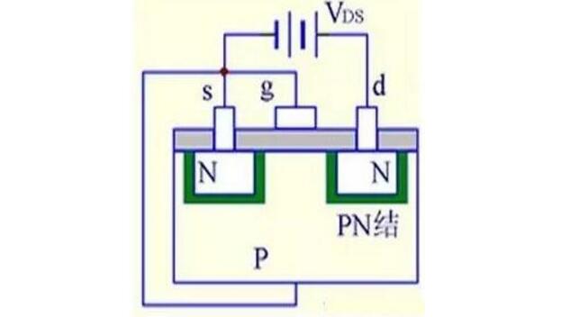
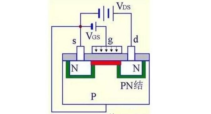
(1) When VGS = 0, there is always a PN junction reverse bias regardless of the polarity of the VDS, so there is no conductive channel.
VGS=0, ID=0
VGS must be greater than 0
The pipe can work.
What is MOS tube? MOS tube structure principle diagram (application _ advantage _ three poles representative)
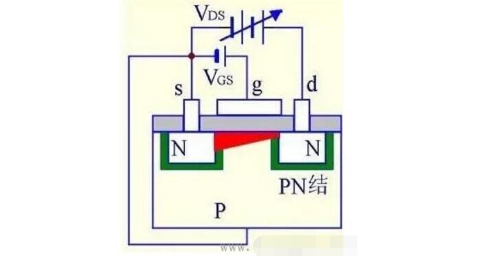
(2) When VGS is 0, an electric field perpendicular to the surface of the semiconductor is generated in the Sio2 medium, and the multi-holes in the P region are repelled to attract the minority electrons. When the VGS reaches a certain value, the surface of the P region will form an inversion layer to communicate the N regions on both sides to form a conductive channel.
VGSˇ·0ˇúg attracts electronˇúinversion layerˇúconductive channel
VGSˇüˇúInverse layer thickeningˇúVDSˇüˇúIDˇü
(3) When VGSˇÝVT and VDS is small:
VDSˇüˇúIDˇü
What is MOS tube? MOS tube structure principle diagram (application _ advantage _ three poles representative)
VT: turn on the voltage, make it in VDS
VGSˇă when starting to conduct electricity
VT=VGSˇŞVDS
What is MOS tube? MOS tube structure principle diagram (application _ advantage _ three poles representative)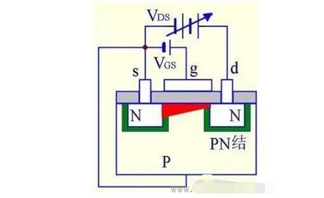
(4) When VGS is 0 and VDS is increased to a certain value, the channel near the drain is pinched off to form a pinch-off region.
VDSˇüˇúID unchanged
What are the three poles of the mos tube and the method of determination?
The three poles of the MOS tube are: G (gate), D (drain) s (source and), and the voltage between the gate and the source is required to be greater than a certain value, and the drain and source are turned on.
What is MOS tube? MOS tube structure principle diagram (application _ advantage _ three poles representative)

1. Judging the gate G
MOS driver mainly plays the role of waveform shaping and enhanced driving: If the G signal waveform of MOS tube is not steep enough, it will cause a lot of power loss in the feedback switching stage. The side effect is to reduce the conversion efficiency of the circuit. The MOS tube has a severe fever and is easy to damage the MOS tube GS. There is a certain capacitance between them. If the driving ability of the G signal is not enough, it will seriously affect the time of waveform jump.
Short-circuit the G-S pole, select the RˇÁ1 file of the multimeter, connect the black meter to the S pole, and the red meter to the D pole. The resistance should be several ohms to ten ohms. If it is found that the resistance of a foot and its feet is infinite, and it is still infinite after exchanging the pen, it is confirmed that this pin is G pole, because it is insulated from the other two pins.
2. Determine source S and drain D
Turn the multimeter to the RˇÁ1k file to measure the resistance between the three pins. The resistance is measured twice by the exchange meter method, wherein the resistance value is low (generally several thousand ohms to ten thousand ohms) and the primary resistance is one time. At this time, the black meter pen is the S pole, and the red meter pen is connected to the D pole. Because of the different test conditions, the measured RDS(on) value is higher than the typical value given in the manual.
3. Measure the drain-source on-state resistance RDS(on)
There is a PN junction between the source and drain, so the S and D poles can be identified based on the difference in the positive and negative resistances of the PN junction. For example, an IRFPC50 VMOS tube is measured with a 500-type multimeter RˇÁ1 file, and RDS(on)=3.2W, which is greater than 0.58W (typical).
Test steps:
The detection of the MOS tube is mainly to judge the leakage, short circuit, open circuit and amplification of the MOS tube.
The steps are as follows:
If there is a resistance value, the MOS tube is not tested for leakage.
1. Remove the resistance between the connection gate and the source, and the red and black pens of the multimeter are unchanged. If the hands are slowly returned to high resistance or infinitely after the resistance is removed, the MOS tube leaks and remains unchanged.
2. Then a wire connects the gate and source of the MOS transistor. If the pointer returns to infinity immediately, the MOS is intact.
3. Connect the red pen to the source S of the MOS. The black pen is connected to the drain of the MOS tube. The good pointer indication should be infinite.
4. Connect a 100K¦¸-200K¦¸ resistor to the gate and drain, then connect the red pen to the source S of the MOS. The black pen is connected to the drain of the MOS transistor. Is 0, at this time, the lower charge charges the gate of the MOS tube through this resistor to generate a gate electric field. Since the electric field is generated, the conductive channel causes the drain and the source to be turned on, so the pointer of the multimeter is deflected, and the angle of deflection is large. The better the discharge.
Application field of MOS tube (field effect tube)
1: Industrial field, stepper motor drive, electric drill tool, industrial switching power supply
2: New energy field, photovoltaic inverter, charging pile, drone
3: Transportation field, car inverter, car HID ballast, electric bicycle
4: Green lighting field, CCFL energy saving lamp, LED lighting power supply, metal halide lamp ballast
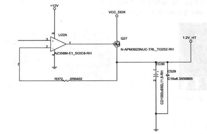
MOS tube step-down circuit
In the figure, Q27 is an N-channel MOS transistor. When U22A's 1 pin outputs a high level, Q27 turns on, and the VCC-DDR memory voltage is stepped down to obtain 1.2V-HT bus power supply. When U22A's 1 pin outputs low level, Q27 is turned off. The 1.2V_HT bus voltage is 0V.