Collect
 NavigateŁş


Allegro A3515 and A3516 datasheet
 DescriptionŁş
 print
print
 telŁş0755-83031813
 emailŁşsumzi@sumzi.com


- Production
- Technology
- Configuration
- Download
ProductionŁş
A3515 and A3516
Ratiometric Linear Hall-Effect Sensors for High-Temperature Operation

These parts are in production but are not recommended for new designs (Not for New Design). This classification is used to restrict business to only those customers presently using the product. The A1321 and A1323devices are intended to replace the A3515/7 and A3516/8 devices respectively. It is recommended that these new devices be considered for all new designs. If the A1321 or A1323 devices do not meet your application's requirements, please contact the local field applications engineer or sales support for alternatives.
Features
- Temperature-Stable Quiescent Output Voltage
- Precise Recoverability After Temperature Cycling
- Output Voltage Proportional to Applied Magnetic Field
- Ratiometric Rail-to-Rail Output
- Improved Sensitivity
- 4.5 V to 5.5 V Operation
- Immune to Mechanical Stress
- Small Package Size
- Solid-State Reliability
Description
The A3515- and A3516- are sensitive, temperature-stable linear Hall-effect sensors with greatly improved offset characteristics. Ratiometric, linear Hall-effect sensors provide a voltage output that is proportional to the applied magnetic field and have a quiescent output voltage that is approximately 50% of the supply voltage. These magnetic sensors are ideal for use in linear and rotary position sensing systems in the harsh environments of automotive and industrial applications over extended temperatures to -40ˇăC and +150ˇăC. The A3515- features an output sensitivity of 5 mV/G, while the A3516- has an output sensitivity of 2.5 mV/G. See the Magnetic Characteristics table for complete, individual device parametrics.
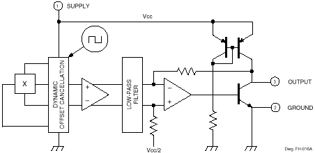
Each BiCMOS monolithic circuit integrates a Hall element, improved temperature-compensating circuitry to reduce the intrinsic sensitivity drift of the Hall element, a small-signal high-gain amplifier, and a rail-to-rail low-impedance output stage.
A proprietary dynamic offset cancelation technique, with an internal high-frequency clock, reduces the residual offset voltage, which is normally caused by device overmolding, temperature dependancies, and thermal stress. This technique produces devices that have an extremely stable quiescent output voltage, are immune to mechanical stress, and have precise recover-ability after temperature cycling. Many problems normally associated with low-level analog signals are minimized by having the Hall element and amplifier in a single chip. Output precision is obtained by internal gain and offset trim adjustments during the manufacturing process.
Functional Block Diagram
| Part Number | Package Type | RoHS | Temperature |
| Compliant | |||
| A3515XUA-CALIB | 3-pin SIP | No | -20 ˇăC to 85 ˇăC |
| A3515EUA | 3-pin SIP | No | -40 ˇăC to 85 ˇăC |
| A3515LUA | 3-pin SIP | No | -40 ˇăC to 150 ˇăC |
| A3516XUA-CALIB | 3-pin SIP | No | -20 ˇăC to 85 ˇăC |
| A3516EUA | 3-pin SIP | No | -40 ˇăC to 85 ˇăC |
| A3516LUA | 3-pin SIP | No | -40 ˇăC to 150 ˇăC |
Contact person:
Frances New
Phone:+86-755-81832961
Fax:+86-755-83299282
Email:sumzi@sumzi.com
MSN:sumzi_frances@msn.com
http://www.sumzi.com