 收藏本站
收藏本站
 当前位置:
当前位置:A3210 技术资料及报价(附PDF文档)
发布时间:2007-09-17 浏览:12006次
DATASHEET PDF
 A3210.pdf
The A3209Ex and A3210Ex integrated circuits are ultra-sensitive, pole
independent Hall-effect switches with a latched digital output. They are
especially suited for operation in battery-operated, hand-held equipment such as
cellular and cordless telephones, pagers, and palmtop computers. 2.5 volt to
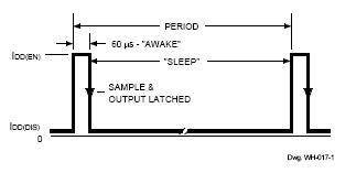
3.5 volt operation and a unique clocking scheme to reduce the average operat-
ing power requirements – the A3209Ex to 400 ?W, the A3210Ex to 25 ?W!
Except for operating duty cycle and average operating current, the A3209Ex
and A3210Ex are identical.
Unlike other Hall-effect switches, either a north or south pole of sufficient
strength will turn the output on; in the absence of a magnetic field, the output is
off. The polarity independence and minimal power requirement allows these
devices to easily replace reed switches for superior reliability and ease of
manufacturing, while eliminating the requirement for signal conditioning.
Improved stability is made possible through chopper stabilization (dynamic
offset cancellation), which reduces the residual offset voltage normally caused
by device overmolding, temperature dependencies, and thermal stress.
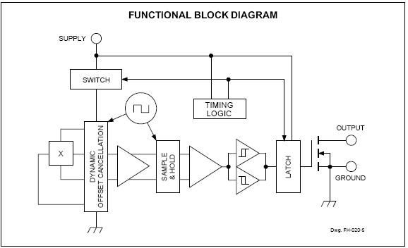
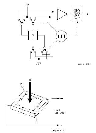
These devices include on a single silicon chip a Hall-voltage generator,
small-signal amplifier, chopper stabilization, a latch, and a MOSFET output.
Advanced BiCMOS processing is used to take advantage of low-voltage and
low-power requirements, component matching, very low input-offset errors,
and small component geometries.
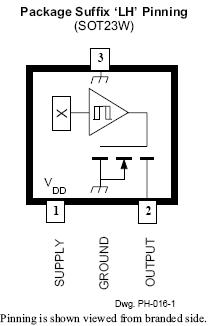
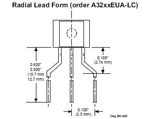
The A3209Ex and A3210Ex are rated for operation over a temperature
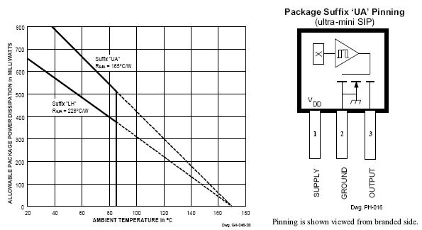
range of -40?C to +85?C. Two package styles provide a magnetically opti-
mized package for most applications. Suffix ‘LH’ is a miniature low-profile
surface-mount package while suffix ‘UA’ is a three-lead ultra-mini-SIP for
through-hole or surface mounting.
FEATURES
■ Micropower Operation
■ Operate With North or South Pole
■ 2.5 V to 3.5 V Battery Operation
■ Chopper Stabilized
Superior Temperature Stability
Extremely Low Switch-Point Drift
Insensitive to Physical Stress
■ ESD Protected to 5 kV
■ Solid-State Reliability
■ Small Size
■ Easily Manufacturable With Magnet Pole Independence
Always order by complete part number: the prefix ‘A’ + the basic four-digit
part number + the suffix ‘E’ to indicate operating temperature range + a
suffix to indicate package style, e.g.,
Chopper-Stabilized Technique. The Hall element can be
considered as a resistor array similar to a Wheatstone bridge. A
large portion of the offset is a result of the mismatching of these
resistors. These devices use a proprietary dynamic offset
cancellation technique, with an internal high-frequency clock to
reduce the residual offset voltage of the Hall element that is
normally caused by device overmolding, temperature dependen-
cies, and thermal stress. The chopper-stabilizing technique
cancels the mismatching of the resistor circuit by changing the
direction of the current flowing through the Hall plate using
CMOS switches and Hall voltage measurement taps, while
maintaing the Hall-voltage signal that is induced by the external
magnetic flux. The signal is then captured by a sample-and-
hold circuit and further processed using low-offset bipolar
circuitry. This technique produces devices that have an
extremely stable quiescent Hall output voltage, are immune to
thermal stress, and have precise recoverability after temperature
cycling. This technique will also slightly degrade the device
output repeatability. A relatively high sampling frequency is
used in order that faster signals can be processed.
More detailed descriptions of the circuit operation can be
found in: Technical Paper STP 97-10, Monolithic Magnetic
Hall Sensor Using Dynamic Quadrature Offset Cancellation
and Technical Paper STP 99-1, Chopper-Stabilized Amplifiers
With A Track-and-Hold Signal Demodulator.
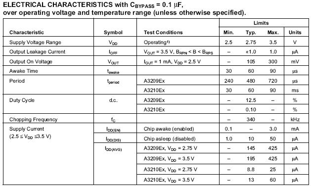
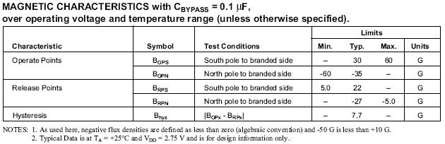
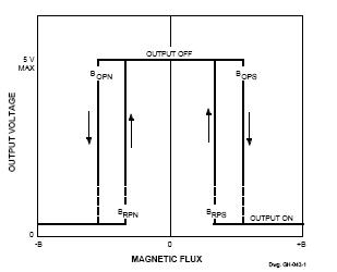
Operation. The output of this device switches low (turns on)
when a magnetic field perpendicular to the Hall sensor exceeds
the operate point BOPS (or is less than BOPN). After turn-on, the
output is capable of sinking up to 1 mA and the output voltage
is VOUT(ON). When the magnetic field is reduced below the
release point BRPS (or increased above BRPN), the device output
switches high (turns off). The difference in the magnetic
operate and release points is the hysteresis (Bhys) of the device.
This built-in hysteresis allows clean switching of the output
even in the presence of external mechanical vibration and
electrical noise.
As used here, negative flux densities are defined as less
than zero (algebraic convention) and -50 G is less than +10 G
上一篇:A3213 and A3214 技术资料及报价(附PDF文档) 2026-06-22
下一篇:MLX90248 技术资料及报价(附PDF文档) 2026-06-22


