|
|
|
• |
|
|
• |
|
|
• |
|
|
• |
|
|
• |
|
 |
| | | | |
|
 |
|
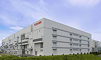
Fab 4 was constructed using the latest earthquake-absorbing structure. |
|
Responding to the rising demand for NAND flashmemory, ToshibaCorp. and SanDiskCorp. have inaugurated a 300mm wafer fab at Toshiba's Yokkaichi Operations in Mie Prefecture, Japan.
The new Fab 4 is expected to start mass production in December and reach a production capacity of 80,000 wafers a month in the second half of 2008. The fab still has space to expand capacity, and further investment could take output to 210,000 wafers per month, in anticipation of increases in future market demand. The new fab will use 56nm process technology at start-up and plans call for a gradual transition to 43nm technology starting March 2008.
Fab 4 is designed to minimize impact of natural disasters on operations. The building was constructed using the latest earthquake-absorbing structure, which is designed to dampen temblor force by up to two-thirds, and deploys multiple power compensation that is triggered instantaneously by any sudden, momentary loss of power supply.
"Fab 4 will feature world-class manufacturing capabilities, both in scale and productivity. It will support us in reinforcing our leadership in the fast-growing global market for higher density NAND flash memories, and provide a powerful engine of growth for both companies," said Shozo Saito, corporate senior VP of Toshiba and president and CEO of Toshiba's semiconductor company.
Eli Harari, CEO and chairman of SanDisk, said, "The enormous size and technology scope of Fab 4 reflect our confidence and optimism for the future, and we believe will enable us to competitively meet the growing demand for flash storage from our global customers in the years ahead."
Toshiba funded construction of the Fab 4 building, and Flash Alliance Ltd, a Toshiba-SanDisk venture established in July 2006, is funding the advanced manufacturing equipmentnow being installed in the fab. |  收藏本站
收藏本站
 当前位置:
当前位置:


