Collect
 Navigate:
A3957SLB 세減꽝鑒섟괩송(맒PDF)
 A3957SLB.pdf
The A3957SLB is designed for driving one winding of a bipolar stepper
motor in a microstepping mode. The outputs are rated for continuous output
currents to ?1.5 A and operating voltages to 50 V. Internal pulse-width
modulated (PWM) current control combined with an internal four-bit nonlin-
ear digital-to-analog converter allows the motor current to be controlled in
full-, half-, quarter-, eighth-, or sixteenth-step (microstepping) modes.
Nonlinear increments minimize the number of control lines necessary for
microstepping. Microstepping provides for increased step resolution, and
reduces torque variations and resonance problems at low speed.
Internal circuitry determines whether the PWM current-control circuitry
operates in a slow (recirculating) current-decay mode, fast (regenerative)
current-decay mode, or in a mixed current-decay mode in which the off time
is divided into a period of fast current decay with the remainder of the fixed
off time spent in slow current decay. The combination of user-selectable
current-sensing resistor and reference voltage, digitally selected output
current ratio; and slow, fast, or mixed current-decay modes provides users
with a broad, variable range of motor control.
Internal circuit protection includes thermal shutdown with hysteresis,
transient-suppression diodes, and crossover current protection. Special
power-up sequencing is not required.
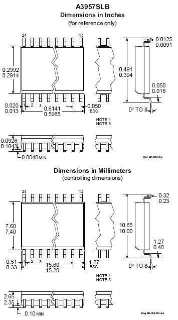
The A3957SLB is supplied in a 24-lead plastic SOIC with copper heat-
sink tabs. The power tab is at ground potential and needs no electrical
isolation.
FEATURES
⊆ ?1.5 A Continuous Output Current
⊆ 50 V Output Voltage Rating
⊆ Internal PWM Current Control
⊆ 4-Bit Non-Linear DAC for 16-Bit Microstepping
⊆ Satlington? Sink Drivers
⊆ Fast, Mixed Fast/Slow, and Slow Current-Decay Modes
⊆ Internal Transient-Suppression Diodes
⊆ Internal Thermal-Shutdown Circuitry
⊆ Crossover-Current and UVLO Protection
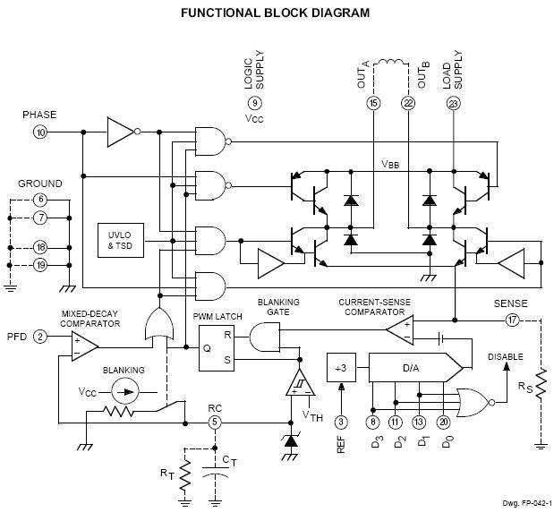
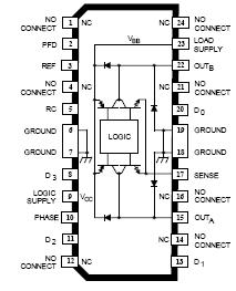
Functional Description
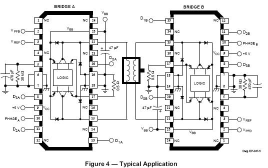
Two A3957SLB full-bridge PWM microstepping motor
drivers are needed to drive the windings of a bipolar stepper
motor. Internal pulse-width modulated (PWM) control circuitry
regulates each motor winding’s current. The peak motor
current is set by the value of an external current-sense resistor
(RS), a reference voltage (VREF), and the digital-to-analog
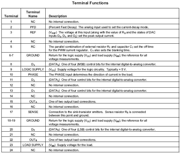
converter (DAC) data inputs (D0, D1, D2, and D3).
To improve motor performance, especially when using
sinusoidal current profiles necessary for microstepping, the
A3957SLB has three distinct current-decay modes: slow decay,
fast decay, and mixed decay.
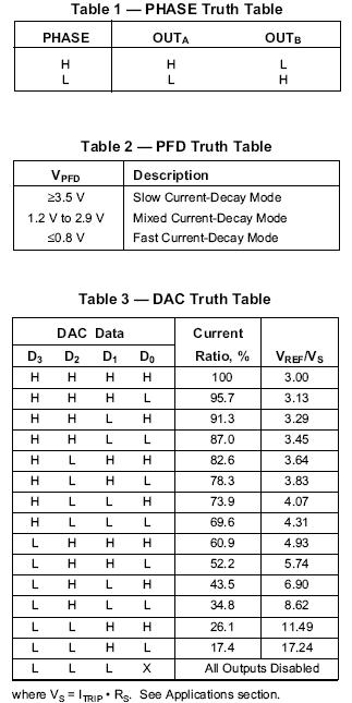
PHASE Input. The PHASE input controls the direction of
current flow in the load (table 1). An internally generated dead
time of approximately 1.5 ?s prevents crossover currents that
could occur when switching the PHASE input.
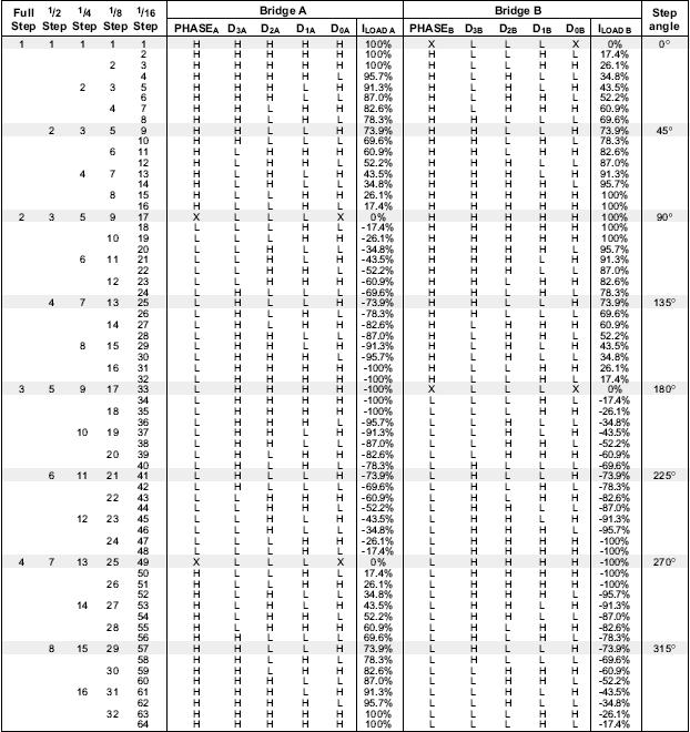
DAC Data Inputs (D0, D1, D2, D3). A non-linear DAC is used
to digitally control the output current. The output of the DAC is
used to set the trip point of the current-sense comparator. Table
3 shows DAC output voltages for each input condition. When
D1, D2, and D3 are all logic low, all of the power output
transistors are turned off.
Internal PWM Current Control. Each motor driver IC
contains an internal fixed off-time PWM current-control circuit
that limits the load current to a desired value (ITRIP). Initially, a
diagonal pair of source and sink transistors are enabled and
current flows through the motor winding and RS (figure 1)
When the voltage across the sense resistor equals the DAC
output voltage, the current-sense comparator resets the PWM
latch, which turns off the source drivers (slow-decay mode) or
the sink and source drivers (fast- or mixed-decay mode).
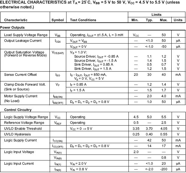
With the DATA input lines tied to VCC, the maximum
value of current limiting is set by the selection of RS and VREF
with a transconductance function approximated by:
ITRIP ≒ VREF/3RS = IOUT + ISO.
where ISO is the sense-current offset due to the base-drive
current of the sink transistor (typically 30 mA). The actual peak
load current (IPEAK) will be slightly higher than ITRIP due to
internal logic and switching delays. The driver(s) remain off
for a time period determined by a user-selected external
resistor-capacitor combination (RTCT). At the end of the fixed
off time, the driver(s) are re-enabled, allowing the load current
to increase to ITRIP again, maintaining an average load current.
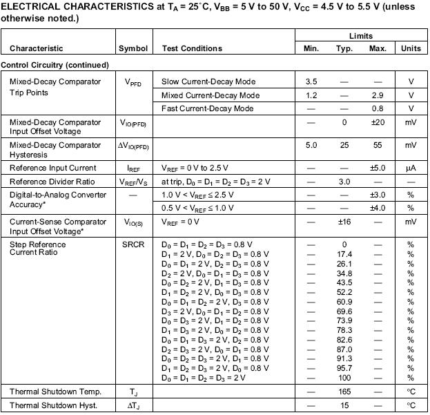
The current-sense comparator has a fixed offset of approxi-
mately 16 mV. With RS = 0.5 ?, the sense-current offset (ISO)
is effectively cancelled (VIO(S) ≒ ISO ? RS).
The DAC data input lines are used to provide up to eight
levels of output current. The internal 4-bit digital-to-analog
converter reduces the reference input to the current-sense
comparator in precise steps (the step reference current ratio or
SRCR) to provide half-step, quarter-step, eighth-step, or
“microstepping” load-current levels.
ITRIP ≒ SRCR x VREF/3RS
Slow Current-Decay Mode. When VPFD◎ 3.5 V, the device is
in slow current-decay mode (the source drivers are disabled
when the load current reaches ITRIP). During the fixed off time,
the load inductance causes the current to recirculate through the
motor winding, sink driver, ground clamp diode, and sense
resistor (see figure 1). Slow-decay mode produces low ripple
current for a given fixed off time (see figure 2). Low ripple
current is desirable because the average current in the motor
winding is more nearly equal to the desired reference value,
resulting in increased motor performance in microstepping
applications.
For a given level of ripple current, slow decay affords the
lowest PWM frequency, which reduces heating in the motor and
driver IC due to a corresponding decrease in hysteretic core
losses and switching losses respectively. Slow decay also has
the advantage that the PWM load current regulation can follow
a more rapidly increasing reference before the PWM frequency
drops into the audible range. For these reasons slow-decay
mode is typically used as long as good current regulation can be
maintained.
Under some circumstances slow-decay mode PWM can fail
to maintain good current regulation:
1) The load current will fail to regulate in slow-decay mode
due to a sufficiently negative back-EMF voltage in con-
junction with the low voltage drop across the load during
slow decay recirculation. The negative back-EMF voltage
can cause the load current to actually increase during the
slow decay off time. A negative back-EMF voltage
condition commonly occurs when driving stepping motors
because the phase lead of the rotor typically causes the
back-EMF voltage to be negative towards the end of each
step (see figure 3A).
2) When the desired load current is decreased rapidly, the
slow rate of load current decay can prevent the current from
following the desired reference value.
3) When the desired load current is set to a very low value,
the current-control loop can fail to regulate due to its
minimum duty cycle, which is a function of the user-
selected value of tOFF and the minimum on-time pulse
width ton(min) that occurs each time the PWM latch is reset.
Fast Current-Decay Mode. When VPFD● 0.8 V, the device is
in fast current-decay mode (both the sink and source drivers are
disabled when the load current reaches ITRIP). During the fixed
off time, the load inductance causes the current to flow from
ground to the load supply via the motor winding, ground-clamp
and flyback diodes (see figure 1). Because the full motor
supply voltage is across the load during fast-decay recirculation,
the rate of load current decay is rapid, producing a high ripple
current for a given fixed off time (see figure 2). This rapid rate
of decay allows good current regulation to be maintained at the
cost of decreased average current accuracy or increased driver
and motor losses
Mixed Current-Decay Mode. If VPFD is between 1.2 V and
2.9 V, the device will be in a mixed current-decay mode.
Mixed-decay mode allows the user to achieve good current
regulation with a minimum amount of ripple current and motor/
driver losses by selecting the minimum percentage of fast decay
required for their application (see also Stepper Motor Applica-
tions).
As in fast current-decay mode, mixed-decay starts with the sink
and source drivers disabled after the load current reaches ITRIP.
When the voltage at the RC terminal decays to a value below
VPFD, the sink drivers are re-enabled, placing the device in slow
current-decay mode for the remainder of the fixed off time
(figure 2). The percentage of fast decay (PFD) is user deter-
mined by VPFD or two external resistors.
PFD = 100 ln (0.6[R1+R2]/R2)
where
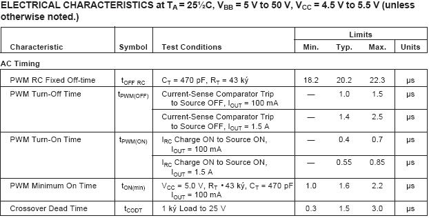
Fixed Off-Time. The internal PWM current-control circuitry
uses a one shot to control the time the driver(s) remain(s) off.
The one-shot off-time, tOFF, is determined by the selection of an
external resistor (RT) and capacitor (CT) connected from the RC
timing terminal to ground. The off-time, over a range of values
of CT = 470 pF to 1500 pF and RT = 12 k? to 100 k?, is
approximated by:
tOFF≒ RTCT.
When the load current is increasing, but has not yet reached
the sense-current comparator threshold (ITRIP), the voltage on
the RC terminal is approximately 0.6VCC. When ITRIP is
reached, the PWM latch is reset by the current-sense compara-
tor and the voltage on the RC terminal will decay until it
reaches approximately 0.22VCC. The PWM latch is then set,
thereby re-enabling the driver(s) and allowing load current to
increase again. The PWM cycle repeats, maintaining the peak
load current at the desired value.
With increasing values of tOFF, switching losses will
decrease, low-level load-current regulation will improve, EMI
will be reduced, the PWM frequency will decrease, and ripple
current will increase. A value of tOFF can be chosen for optimi-
zation of these parameters. For applications where audible
noise is a concern, typical values of tOFF are chosen to be in the
range of 15 ?s to 35 ?s.
RC Blanking. In addition to determining the fixed off-time of
the PWM control circuit, the CTcomponent sets the comparator
blanking time. This function blanks the output of the current-
sense comparator when the outputs are switched by the internal
current-control circuitry (or by the PHASE input, or when the
device is enabled with the DAC data inputs). The comparator
output is blanked to prevent false over-current detections due to
reverse recovery currents of the clamp diodes, and/or switching
transients related to distributed capacitance in the load.
During internal PWM operation, at the end of the tOFF time,
the comparator’s output is blanked and CT begins to be charged
from approximately 0.22VCC by an internal current source of
approximately 1 mA. The comparator output remains blanked
until the voltage on CT reaches approximately 0.6VCC. The
blanking time, tBLANK, can be calculated as:
tBLANK = RTCT ln (RT/[RT - 3 k?]).
When a transition of the PHASE input occurs, CT is
discharged to near ground during the crossover delay time (the
crossover delay time is present to prevent simultaneous conduc-
tion of the source and sink drivers). After the crossover delay,
CT is charged by an internal current source of approximately 1
mA. The comparator output remains blanked until the voltage
on CT reaches approximately 0.6VCC.
Similarly, when the device is disabled, via the DAC data
inputs, CT is discharged to near ground. When the device is re-
enabled, CT is charged by an internal current source of approxi-
mately 1 mA. The comparator output remains blanked until the
voltage on CT reaches approximately 0.6VCC. The blanking
time, tBLANK▽, can be calculated as:
tBLANK▽?≒ 1900 CT.
The minimum recommended value for CT is 470 pF
? 5 %. This value ensures that the blanking time is sufficient to
avoid false trips of the comparator under normal operating
conditions. For optimal regulation of the load current, this
value for CT is recommended and the value of RT can be sized
to determine tOFF.
Thermal Considerations. Thermal-protection circuitry turns
off all output transistors when the junction temperature reaches
approximately +165?C. This is intended only to protect the
device from failures due to excessive junction temperatures and
should not imply that output short circuits are permitted. The
output transistors are re-enabled when the junction temperature
cools to approximately +150?C.
Stepper Motor Applications. The A3957SLB is used to
optimize performance in microstepping/sinusoidal stepper-
motor drive applications (see figures 4 and 5). When the load
current is increasing, the slow current-decay mode is used to
limit the switching losses in the driver and iron losses in the
motor. This also improves the maximum rate at which the load
current can increase (as compared to fast decay) due to the slow
rate of decay during tOFF. When the load current is decreasing,
the mixed current-decay mode is used to regulate the load
current to the desired level. This prevents tailing of the current
profile caused by the back-EMF voltage of the stepper motor
(see figure 3A).
璂송훑窟:
0755-83283733, 83031813,33062500
QQ:623069669
MSN:sumzi003@sumzi.com sumzi006@sumzi.com
Email:sumzi@sumzi.com
http://www.sumzi.com
Pre:Samsung Electro-Mechanics랙꼈0603룐陋돨1uF MLCC 2026-02-05
Next:A3966 세減꽝鑒 2026-02-05