 收藏本站
收藏本站
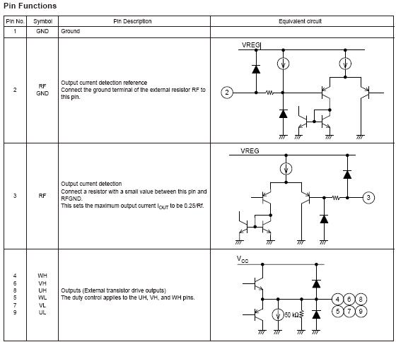
 当前位置:
当前位置:LB11696V 详细规格书及技术资料和报价(附PDF文档)
DATASHEET PDF 696.pdf
The LB11696V is a direct PWM drive predriver IC designed for three-phase power brushless motors. A motor driver
circuit with the desired output power (voltage and current) can be implemented by adding discrete transistors in the
output circuits. Furthermore, the LB11696V provides a full complement of protection circuits allowing it to easily
implement high-reliability drive circuits. This device is optimal for driving all types of large-scale motors such as those
used in air conditioners and on-demand water heaters.
Functions and Features
. Three-phase bipolar drive
. Direct PWM drive (controlled either by control voltage or PWM variable duty pulse input)
. Built-in forward/reverse switching circuit
. Start/stop mode switching circuit (stop mode power saving function)
. Built-in input amplifier
. 5 V regulator output (VREG pin)
. Current limiter circuit (Supports 0.25 V (typical) reference voltage sensing based high-precision detection)
. Undervoltage protection circuit (The operating voltage can be set with a zener diode)
. Automatic recovery type constraint protection circuit with protection operating state discrimination output (RD pin)
. Four types of Hall signal pulse outputs
. Supports thermistor based thermal protection of the output transistors
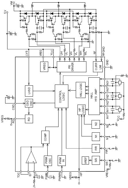
LB11696V Functional Description
1. Output Drive Circuit
LB11696V
The LB11696V adopts direct PWM drive to minimize power loss in the outputs. The output transistors are always
saturated when on, and the motor drive power is adjusted by changing the on duty of the output. The output PWM
switching is performed on the UH, VH, and WH outputs. Since the UL to WL and UH to WH outputs have the same
output form, applications can select either low side PWM or high side PWM drive by changing the way the external
output transistors are connected. Since the reverse recovery time of the diodes connected to the non-PWM side of
the outputs is a problem, these devices must be selected with care. (This is because through currents will flow at the
instant the PWM side transistors turn on if diodes with a short reverse recovery time are not used.)
2. Current Limiter Circuit
The current limiter circuit limits the output current peak value to a level
determined by the equation I = VFR/Rf (VRF = 0.25 V typical, Rf:
current detection resistor). This circuit suppresses the output current by
reducing the output on duty.
High-precision detection can be implemented by connecting the lines
from the RF and RFGND pins close to the two terminal of the current
detection resistor Rf.
To the RF pin
Current
detection
resistor
The current limiter circuit includes an internal filter circuit to prevent incorrect current limiter circuit operation due
to detecting the output diode reverse recovery current due to PWM operation. Although there should be no problems
with the internal filter circuit in normal applications, applications should add an external filter circuit (such as an RC
low-pass filter) if incorrect operation occurs (if the diode reverse recovery current flows for longer than
1 µs).
3. Power Saving Circuit
This IC goes to a low-power mode (power saving state) when set to the
stop state with the S/S pin. In the power saving state, the bias currents in
most of the circuits are cut off. However, the 5 V regulator output
(VREG) is still provided in the power saving state. If it is also necessary
to cut the Hall device bias current, this function can be provided by an
application that, for example, connects the Hall devices to 5 V through
PNP transistors.
4. Notes on the PWM Frequency
The PWM frequency is determined by the capacitor C (F) connected to the PWM pin.
fPWM≈ 1/(22500 × C)
If a 2000 pF capacitor is used, the circuit will oscillate at about 22 kHz. If the PWM frequency is too low, switching
noise will be audible from the motor, and if it is too high, the output power loss will increase. Thus a frequency in
the range 15 to 50 kHz must be used. The capacitor's ground terminal must be placed as close as possible to the IC’s
ground pin to minimize the influence of output noise and other noise sources.
5. Control Methods
The output duty can be controlled by either of the following methods
• Control based on comparing the TOC pin voltage to the PWM oscillator waveform
The low side output transistor duty is determined according to the result of comparing the TOC pin voltage to the
PWM oscillator waveform. When the TOC pin voltage is 1.35 V or lower, the duty will be 0%, and when it is 3.0
V or higher, the duty will be 100%.
Since the TOC pin is the output of the control amplifier (CTL), a control voltage cannot be directly input to the
TOC pin. Normally, the control amplifier is used as a full feedback amplifier (with the EI- pin connected to the
TOC pin) and a DC voltage is input to the EI+ pin (the EI+ pin voltage will become equal to the TOC pin voltage).
When the EI+ pin voltage becomes higher, the output duty increases. Since the motor will be driven when the EI+
pin is in the open state, a pull-down resistor must be connected to the EI+ pin if the motor should not operate when
EI+ is open.
When TOC pin voltage control is used, a low-level input must be applied to the PWMIN pin or that pin connected
to ground.
• Pulse Control Using the PWMIN Pin
LB11696V
A pulse signal can be input to the PWMIN pin, and the output can be controlled based on the duty of that signal.
Note that the output is on when a low level is input to the PWMIN pin, and off when a high level is input. When
the PWMIN pin is open it goes to the high level and the output is turned off. If inverted input logic is required,
this can be implemented with an external transistor (npn).
When controlling motor operation from the PWMIN pin, the EI– pin must be connected to ground, and the EI+
pin must be connected to the TOC pin.
Note that since the PWM oscillator is also used as the clock for internal circuits, a capacitor (about 2000 pF) must
be connected to the PWM pin even if the PWMIN pin is used for motor control.
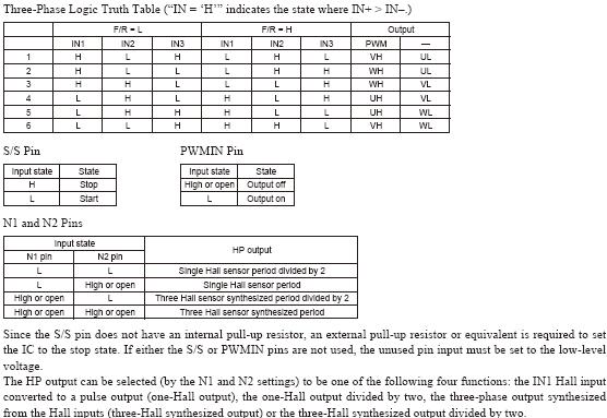
6. Hall Input Signals
A signal input with an amplitude in excess of the hysteresis (80 mV maximum) is required for the Hall inputs.
Considering the possibility of noise and phase displacement, an even larger amplitude is desirable.
If disruptions to the output waveforms (during phase switching) or to the HP output (Hall signal output) occur due to
noise, this must be prevented by inserting capacitors across the inputs. The constraint protection circuit uses the Hall
inputs to discriminate the motor constraint state. Although the circuit is designed to tolerate a certain amount of
noise, care is required when using the constraint protection circuit.
If all three phases of the Hall input signal system go to the same input state, the outputs are all set to the off state
(the UL, VL, WL, UH, VH, and WH outputs all go to the low level).
If the outputs from a Hall IC are used, fixing one side of the inputs (either the + or – side) at a voltage within the
common-mode input voltage range allows the other input side to be used as an input over the 0 V to VCCrange.
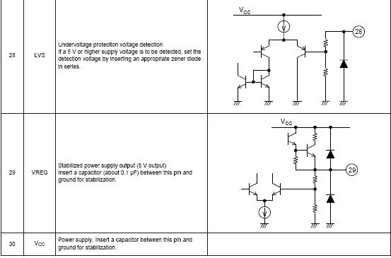
7. Undervoltage Protection Circuit
The undervoltage protection circuit turns one side of the outputs (UH, VH, and WH) off when the LVS pin voltage
falls below the minimum operation voltage (see the Electrical Characteristics). To prevent this circuit from
repeatedly turning the outputs on and off in the vicinity of the protection
operating voltage, this circuit is designed with hysteresis. Thus the output
will not recover until the operating voltage rises 0.45 V (typical).
The protection operating voltage detection level is set up for 5 V systems.
The detected voltage level can be increased by shifting the voltage by
inserting a zener diode in series with the LVS pin to shift the detection
level. The LVS influx current during detection is about 75 µA. To
increase the diode current to stabilize the zener diode voltage rise, insert
a resistor between the LVS pin and ground.
To the power
supply detected
To the LVS pin
If the LVS pin is left open, the internal pull-down resistor will result in the IC seeing a ground level input, and the
output will be turned off. Therefore, a voltage in excess of the LVS circuit clear voltage (about 4.35 V) must be
applied to the LVS pin if the application does not use the undervoltage protection circuit. The maximum rating for
the LVS pin applied voltage is 18 V.
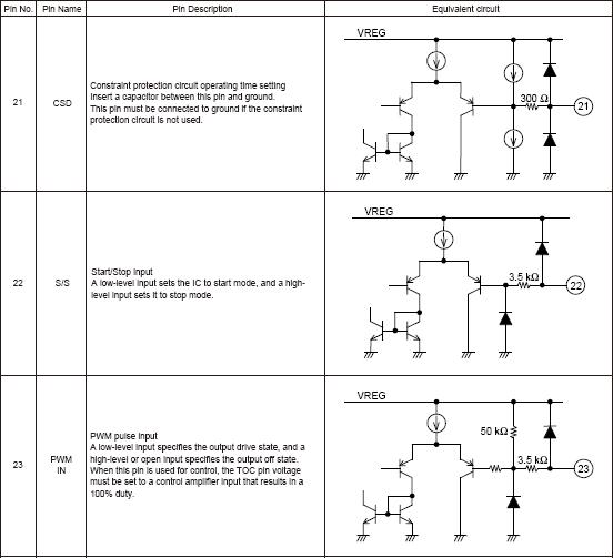
8. Constraint Protection Circuit
When the motor is physically constrained (held stopped), the CSD pin external capacitor is charged (to about 3.0 V)
by a constant current of about 2.5 µA and is then discharged (to about 1.0 V) by a constant current of about 0.14 µA.
This process is repeated, generating a sawtooth waveform. The constraint protection circuit turns motor drive on and
off repeatedly based on this sawtooth waveform. (The UH, VH, and WH side outputs are turned on and off.) Motor
drive is on during the period the CSD pin external capacitor is being charged from about 1.0 V to about 3.0 V, and
motor drive is off during the period the CSD pin external capacitor is being discharged from about 3.0 V to about
1.0 V. The IC and the motor are protected by this repeated drive on/off operation when the motor is physically
constrained.
The motor drive on and off times are determined by the value of the connected capacitor C (in µF).
TCSD1 (drive on period) ≈ 0.8 × C (seconds)
TCSD2 (drive off period) ≈ 14.3 × C (seconds)
When a 0.47 µF capacitor is connected externally to the CSD pin, this iterated operation will have a drive on period
of about 0.38 seconds and a drive off period of about 6.7 seconds.
While the motor is turning, the discharge pulse signal (generated once for each Hall input period) that is created by
combining the Hall inputs internally in the IC discharges the CSD pin external capacitor. Since the CSD pin voltage
does not rise, the constraint protection circuit does not operate.
When the motor is physically constrained, the Hall inputs do not change and the discharge pulses are not generated.
As a result, the CSD pin external capacitor is charged by a constant current of 2.5 µA to about 3.0 V, at which point
the constraint protection circuit operates. When the constraint on the motor is released, the constraint protection
function is released.
Connect the CSD pin to ground if the constraint protection circuit is not used.
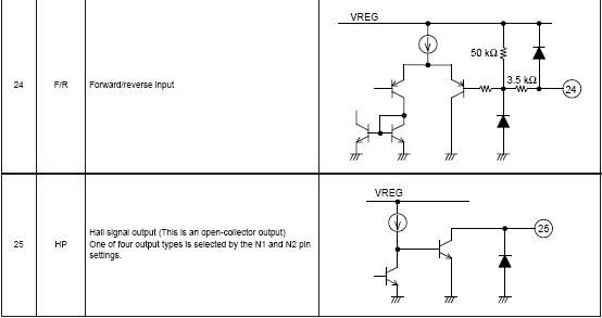
9. Forward/Reverse Direction Switching
This IC is designed so that through currents (due to the output transistor off delay time when switching) do not flow
in the output when switching directions when the motor is turning. However, if the direction is switched when the
motor is turning, current levels in excess of the current limiter value may flow in the output transistors due to the
motor coil resistance and the motor back EMF state when switching. Therefore, designers must consider selecting
external output transistors that are not destroyed by those current levels or only switching directions after the speed
has fallen below a certain speed.
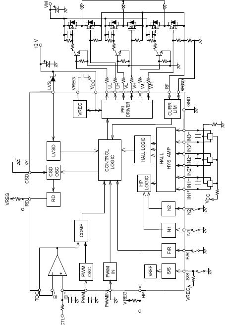
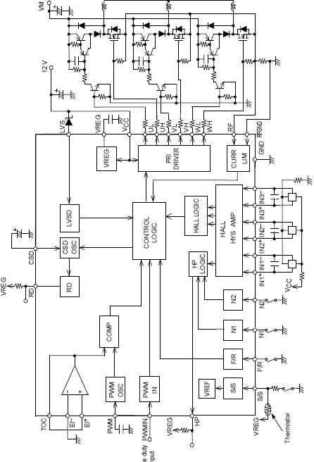
10. Handling Different Power Supply Types
When this IC is operated from an externally supplied 5 V power supply (4.5 to 5.5 V), short the VCCpin to the
VREG pin and connect them to the external power supply.
When this IC is operated from an externally supplied 12 V power supply (8 to 17 V), connect the VCCpin to the
power supply. (The VREG pin will generate a 5 V level to function as the control circuit power supply.)
11. Power Supply Stabilization
Since this IC uses a switching drive technique, the power supply line level can be disturbed easily. Therefore
capacitors with adequate capacitance to stabilize the power supply line must be inserted between VCCand ground.
If diodes are inserted in the power supply lines to prevent destruction if the power supply is connected with reverse
polarity, the power supply lines are even more easily disrupted, and even larger capacitors are required.
If the power supply is turned on and off by a switch, and if there is a significant distance between that switch and the
stabilization capacitor, the supply voltage can be disrupted significantly by the line inductance and surge current into
the capacitor. As a result, the withstand voltage of the device may be exceeded. In application such as this, the surge
current must be suppressed and the voltage rise prevented by not using ceramic capacitors with a low series
impedance, and by using electrolytic capacitors instead.
12. VREG Stabilization
To stabilize the VREG voltage, which is the control circuit power supply, a 0.1 µF or larger capacitor must be
inserted between the VREG pin and ground. The ground side of this capacitor must connected to the IC ground pin
with a line that is as short as possible.

上一篇:TA8428K(S) 技术资料及报价(附PDF文档) 2026-06-14
下一篇:LB1838M 技术资料及报价(附PDF文档) 2026-06-14


